Deltronic Crystal Industries, Inc.

Periodically Poled Lithium Niobate (PPLN)

Applications:

  • Infrared (IR) and mid-IR laser generation
  • Infrared countermeasure and jamming systems
  • Visible wavelength generation
  • First-order and higher-order quasi-phase-matched conversion
  • Remote sensing and spectroscopy

Flexible, Cost-Effective Wavelength Conversion for Visible & Infrared Applications

Periodically Poled Lithium Niobate (PPLN) chips provide a highly efficient and cost-effective solution for visible and mid-infrared wavelength generation. By permanently modifying the nonlinear properties of lithium niobate through a precision-controlled lithographic and electric-field poling process, PPLN enables reliable and repeatable wavelength conversion across a wide spectral range.

This versatility allows engineers to achieve high conversion efficiency while simplifying optical design and reducing overall system cost.

Built for R&D. Proven for Production.

Technical Overview

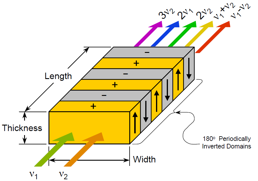
Periodically Poled Lithium Niobate (PPLN) is a nonlinear optical material engineered for efficient wavelength conversion across the visible, infrared (IR), and mid-infrared spectral regions. PPLN chips are fabricated using a multi-step lithographic patterning process followed by precision electric-field poling, resulting in a permanent inversion of ferroelectric domains within the lithium niobate crystal.

This domain inversion enables quasi-phase matching (QPM), allowing nonlinear optical interactions without angular tuning or birefringent phase matching constraints. By selecting appropriate grating periods, crystal widths, and interaction lengths, PPLN supports optimized first-order and higher-order nonlinear processes, including sum-frequency generation (SFG) and difference-frequency generation (DFG).

PPLN offers high nonlinear conversion efficiency, particularly when driven by low peak-power laser sources, making it well suited for compact and power-efficient optical systems. The availability of single and multiple grating configurations enables broadband operation, wavelength tunability, and multi-channel conversion within a single device.

Key Features and Benefits

  • Quasi-phase-matched nonlinear frequency conversion
  • Broad spectral coverage with precise wavelength control
  • High conversion efficiency at low peak power
  • Design flexibility through selectable grating periods and chip geometries
  • Enables compact, lightweight designs for portable and embedded systems
  • Single-grating and multi-grating device options

Specifications

Chip Thickness (standard)

0.5mm and 1.0mm

Chip Width (standard)

5.0mm and 10.0mm (custom up to 40mm)

Chip Length (standard)

10, 20, 30, 40, 50mm (custom up to 60mm)

Single Grating Periods

Many periods available in the range 6.7 to 100+ µm
(plus custom periods)

Multiple Grating Periods

Many multiple grating designs available

Fan-out QPM

To customer specifications

Type I and Type II Phase Matching

To customer specifications

AR Optical Coatings

double band, triple band, broadband

Parallelism (arc min)

< 10 (custom < 1)

Flatness

λ/10

Scratch/Dig

10/5

Material Property - LiNbO3

Transparency Range

330nm – 5500nm

Refractive Index

2.2

Nonlinearity

d21= -2.6pm/V
d31= -4.6pm/V
d33= 25pm/V

Surface Damage Threshold for 10ns (J/cm2)

10

Phasematching Schemes

QPM

* The above figures are based on wavelength at 1064nm and software “SNLO”

Why Choose PPLN?

PPLN combines performance, flexibility, and cost efficiency in a single platform—allowing designers to tailor wavelength conversion to specific system requirements while maintaining high efficiency and compact form factors. It is an ideal solution for applications ranging from laboratory research to field-deployed optical systems.

Contact us to discuss specifications, custom requirements, or production volumes.

Call us at (973) 361-2222 or (973) 328-7000, or click here to contact us.